Characterization of Materials
Characterization, when used in materials science, refers to the use of external techniques to probe into the internal structure and properties of a material. Characterization can take the form of actual materials testing, or analysis, for example in some form of microscope.

The dependence of macroscopic product properties on the characteristics of the material on a microscopic level is another important aspect for successful product development and for the solution of production and quality problems.
Analysis techniques are used simply to magnify the specimen, to visualize its internal structure, and to gain knowledge as to the distribution of elements within the specimen and their interactions.
Magnification and internal visualisation are normally done in a type of microscope, such as :
- Optical Microscope
- Scanning Electron Microscope (SEM)
- Transmission Electron Microscope (TEM)
- Field Ion Microscope (FIM)
- Scanning Tunneling Microscope (STM)
- Atomic Force Microscope (AFM)
Elemental analysis of the specimen can also be done in a number of ways :
- Energy-Dispersive X-ray spectroscopy (EDX)
- Wavelength Dispersive X-ray spectroscopy (WDX)
- Mass spectrometryImpulse excitation technique (IET)
- Secondary Ion Mass Spectrometry (SIMS)
- Electron Energy Loss Spectroscopy (EELS)
- Auger electron spectroscopyX-ray photoelectron spectroscopy (XPS)
Optical Microscope
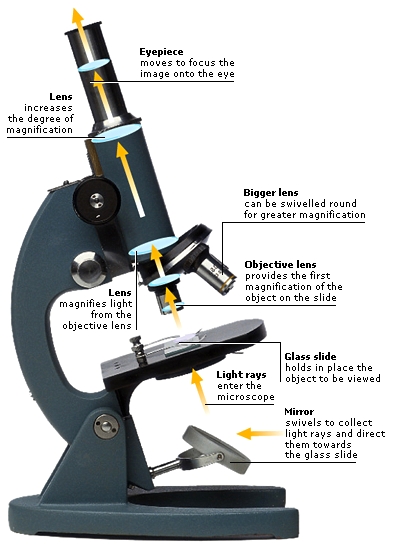
A microscope is an instrument used to see objects too small for the naked eye. The science of investigating small objects using such an instrument is called microscopy. Microscopic means invisible to the eye unless aided by a microscope. The first microscope to be developed was the optical microscope, although the original inventor is not easy to identify. An early microscope was made in 1590 in Middelburg, Netherlands. Two eyeglass makers are variously given credit : Hans Lippershey (who developed an early telescope) and Hans Janssen. Giovanni Faber coined the name microscope for Galileo Galilei’s compound microscope in 1625 (Galileo had called it the “occhiolino” or “little eye”).
Scanning Electron Microscope (SEM)
 A scanning electron microscope (SEM)
A scanning electron microscope (SEM) is a type of electron microscope that images a sample by scanning it with a high-energy beam of electrons in a raster scan pattern. The electrons interact with the atoms that make up the sample producing signals that contain information about the sample’s surface topography, composition, and other properties such as electrical conductivity.
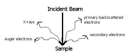
The SEM is an instrument that produces a largely magnified image by using electrons instead of light to form an image. A beam of electrons is produced at the top of the microscope by an electron gun. The electron beam follows a vertical path through the microscope, which is held within a vacuum. The beam travels through electromagnetic fields and lenses, which focus the beam down toward the sample. Once the beam hits the sample, electrons and X-rays are ejected from the sample.
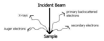
Detectors collect these X-rays, backscattered electrons, and secondary electrons and convert them into a signal that is sent to a screen similar to a television screen. This produces the final image.
Transmission Electron Microscope (TEM)
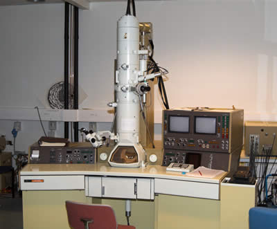
Transmission electron microscopy (TEM)
Transmission electron microscopy (TEM) is a microscopy technique whereby a beam of electrons is transmitted through an ultra thin specimen, interacting with the specimen as it passes through. An image is formed from the interaction of the electrons transmitted through the specimen; the image is magnified and focused onto an imaging device, such as a fluorescent screen, on a layer of photographic film, or to be detected by a sensor such as a CCD camera.
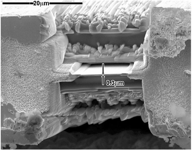 SEM image of a thin TEM sample milled by FIB. The thin membrane shown here is suitable for TEM examination. However, at 300-nm thick, it would not be suitable for high-resolution TEM without further milling.
TEMs are capable of imaging at a significantly higher resolution than light microscopes, owing to the small de Broglie wavelength of electrons. This enables the instrument’s user to examine fine detail—even as small as a single column of atoms, which is tens of thousands times smaller than the smallest resolvable object in a light microscope.
TEM forms a major analysis method in a range of scientific fields, in both physical and biological sciences. TEMs find application in cancer research, virology, materials science as well as pollution, nanotechnology, and semiconductor research.
Field Ion Microscope (FIM)
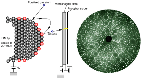
Principle of field ion microscope (FIM)
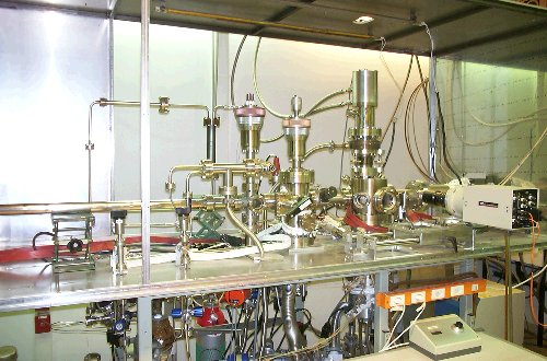
The Field Ion Microscope (FIM) is placed in a home-built all-metal UHV chamber connected to a reaction chamber via a sample transfer system (right-hand).
Field ion microscope (FIM) was invented by Erwin E. Mueller in 1951 at the Pennsylvania State University. By FIM, man observed atoms for the first time. It was developed from its forefunner, the field emission microscpe. The instrument features a specimen in the form of a sharp needle mounted on a electrically insulated stage that is cooled to cryogenic temperatures (20 to 100K) in a ultrahigh vacuum chamber. The field ion image of the specimen is formed on a microchannel plate and phosphor screen assembly that is positioned approximately 50 mm in front of the specimen. To produce a field ion image, controlled amounts of image gas are admitted into the vacuum system. The type of image gas used depends on the material under investigation, common images gases are neon, helium, hydrogen and argon.
Scanning Tunneling Microscope (STM)
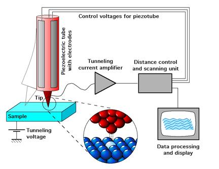
Schematic view of an STM
A scanning tunneling microscope (STM) is an instrument for imaging surfaces at the atomic level. Its development in 1981 earned its inventors, Gerd Binnig and Heinrich Rohrer (at IBM Zürich), the Nobel Prize in Physics in 1986. For an STM, good resolution is considered to be 0.1 nm lateral resolution and 0.01 nm depth resolution. With this resolution, individual atoms within materials are routinely imaged and manipulated. The STM can be used not only in ultra high vacuum but also in air, water, and various other liquid or gas ambients, and at temperatures ranging from near zero kelvin to a few hundred degrees Celsius.
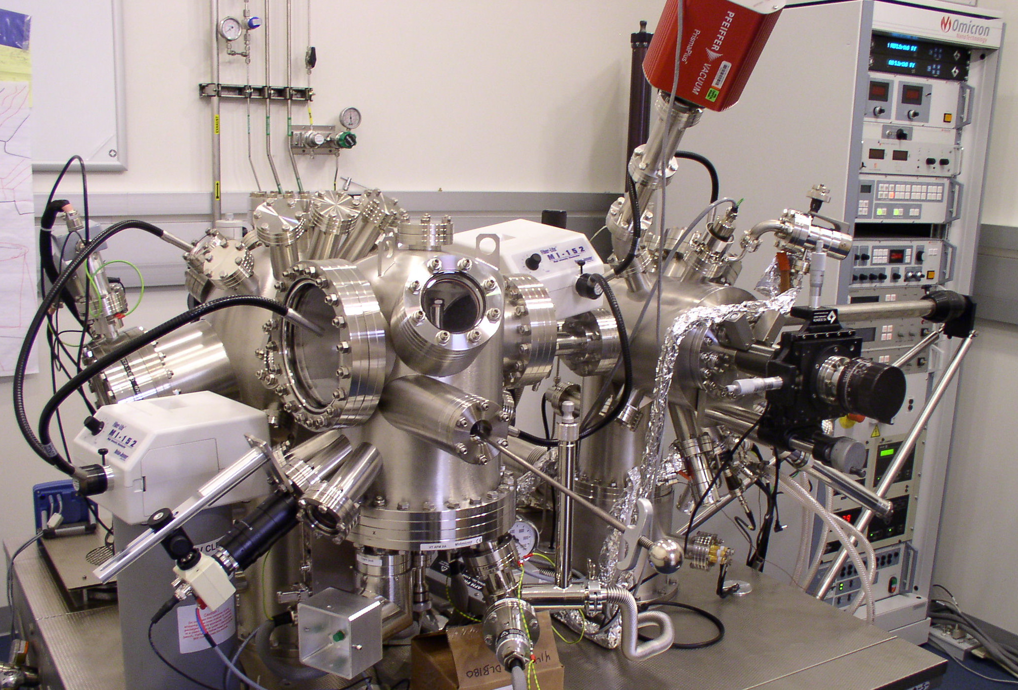
A scanning tunneling microscope (STM) is an instrument for imaging surfaces at the atomic level.
STM is based on the concept of quantum tunneling. When a conducting tip is brought very near to the surface to be examined, a bias (voltage difference) applied between the two can allow electrons to tunnel through the vacuum between them. The resulting tunneling current is a function of tip position, applied voltage, and the local density of states (LDOS) of the sample. Information is acquired by monitoring the current as the tip’s position scans across the surface, and is usually displayed in image form. STM can be a challenging technique, as it requires extremely clean and stable surfaces, sharp tips, excellent vibration control, and sophisticated electronics.
Atomic force microscopy (AFM)
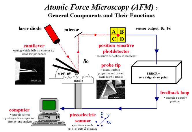
Atomic force microscopy (AFM)
Atomic force microscopy (AFM) or scanning force microscopy (SFM) is a very high-resolution type of scanning probe microscopy, with demonstrated resolution on the order of fractions of a nanometer, more than 1000 times better than the optical diffraction limit. The precursor to the AFM, the scanning tunneling microscope, was developed by Gerd Binnig and Heinrich Rohrer in the early 1980s at IBM Research - Zurich, a development that earned them the Nobel Prize for Physics in 1986. Binnig, Quate and Gerber invented the first atomic force microscope (also abbreviated as AFM) in 1986. The first commercially available atomic force microscope was introduced in 1989.
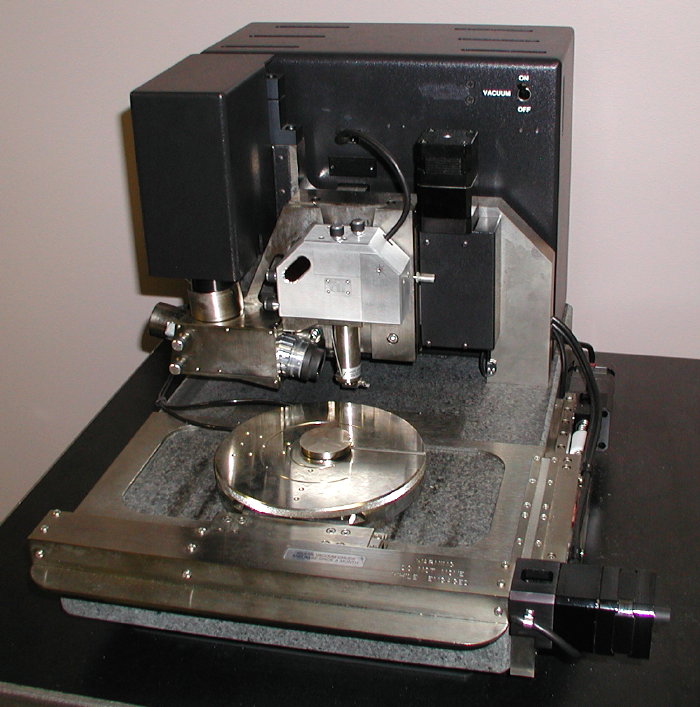
Atomic force microscopy (AFM) is a very high-resolution type of scanning probe microscopy.
The AFM is one of the foremost tools for imaging, measuring, and manipulating matter at the nanoscale. The information is gathered by “feeling” the surface with a mechanical probe. Piezoelectric elements that facilitate tiny but accurate and precise movements on (electronic) command enable the very precise scanning. In some variations, electric potentials can also be scanned using conducting cantilevers. In newer more advanced versions, currents can even be passed through the tip to probe the electrical conductivity or transport of the underlying surface, but this is much more challenging with very few research groups reporting reliable data.


 Alloy Suppliers
  Aluminum
  Aluminum Extrusions
  Copper-Brass-Bronze
  Nickel
  Magnets
  Stainless Steel
  Stainless Steel Tubing
  Steel Service Centers
  Titanium
  Tungsten
  Wire Rope