Advanced Materials : Thin Films
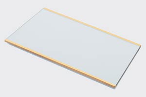
Thin film materials are high purity materials and chemicals used to form or modify thin film deposits and substrates. Examples include precursor gases, sputtering targets, and evaporation filaments. A thin film is a layer of material ranging from fractions of a nanometer (monolayer) to several micrometers in thickness. Electronic semiconductor devices and optical coatings are the main applications benefiting from thin film construction.
Thin Films
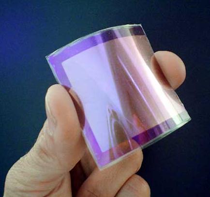
Thin films play an important role in many technological applications including microelectronic devices, magnetic storage media and surface coatings. A familiar application of thin films is the household mirror, which typically has a thin metal coating on the back of a sheet of glass to form a reflective interface.
The performance of optical coatings (e.g. antireflective, or AR, coatings) are typically enhanced when the thin film coating consists of multiple layers having varying thicknesses and refractive indices.
Similarly, a periodic structure of alternating thin films of different materials may collectively form a so-called superlattice which exploits the phenomenon of quantum confinement by restricting electronic phenomena to two-dimensions.
Work is being done with ferromagnetic and ferroelectric thin films for use as computer memory.
It is also being applied to pharmaceuticals, via thin film drug delivery. Thin-films are used to produce thin-film batteries. Thin film application also be adopted on Dye-sensitized solar cell. Ceramic thin films are in wide use. The relatively high hardness and inertness of ceramic materials make this type of thin coating of interest for protection of substrate materials against corrosion, oxidation and wear. In particular, the use of such coatings on cutting tools can extend the life of these items by several orders of magnitude.
Chemical deposition
Here, a fluid precursor undergoes a chemical change at a solid surface, leaving a solid layer. An everyday example is the formation of soot on a cool object when it is placed inside a flame. Since the fluid surrounds the solid object, deposition happens on every surface, with little regard to direction; thin films from chemical deposition techniques tend to be conformal, rather than directional.
Chemical deposition is further categorized by the phase of the precursor :
- Plating relies on liquid precursors, often a solution of water with a salt of the metal to be deposited. Some plating processes are driven entirely by reagents in the solution (usually for noble metals), but by far the most commercially important process is electroplating. It was not commonly used in semiconductor processing for many years, but has seen a resurgence with more widespread use of chemical-mechanical polishing techniques.
- Chemical solution deposition (CSD) uses a liquid precursor, usually a solution of organometallic powders dissolved in an organic solvent. This is a relatively inexpensive, simple thin film process that is able to produce stoichiometrically accurate crystalline phases. This technique is also known as the sol-gel method because the ‘sol’ (or solution) gradually evolves towards the formation of a gel-like diphasic system.
- Chemical vapor deposition (CVD) generally uses a gas-phase precursor, often a halide or hydride of the element to be deposited. In the case of MOCVD, an organometallic gas is used. Commercial techniques often use very low pressures of precursor gas.
- Plasma enhanced CVD (PECVD) uses an ionized vapor, or plasma, as a precursor. Unlike the soot example above, commercial PECVD relies on electromagnetic means (electric current, microwave excitation), rather than a chemical reaction, to produce a plasma.
Research is being done on a new class of thin film inorganic oxide materials, called amorphous heavy-metal cation multicomponent oxides, which could be used to make transparent transistors that are inexpensive and stable.
Any technique that deposits a thin film material onto a substrate or previously deposited layers is considered thin-film deposition. “Thin” generally implies micro, nano, or atomic scales for characterizing deposited layers. Thin-film deposition can be specified as either chemical or physical deposition depending on the means by which the layer is deposited.
Thin film materials function in a variety of ways. Using a precursor gas method involves providing a metal-containing precursor to an activation zone, and activating the metal-containing precursor to form an activated precursor. The activated precursor gas is moved to a reaction chamber, and a film is deposited on a substrate using a cyclical deposition process, wherein the activated precursor gas and a reducing gas are alternately adsorbed onto the substrate.
Physical deposition
Physical deposition uses mechanical, electromechanical or thermodynamic means to produce a thin film of solid. An everyday example is the formation of frost. Since most engineering materials are held together by relatively high energies, and chemical reactions are not used to store these energies, commercial physical deposition systems tend to require a low-pressure vapor environment to function properly most can be classified as physical vapor deposition (PVD).
A thin film is a layer of material ranging from fractions of a nanometer (monolayer) to several micrometers in thickness
The material to be deposited is placed in an energetic, entropic environment, so that particles of material escape its surface. Facing this source is a cooler surface which draws energy from these particles as they arrive, allowing them to form a solid layer. The whole system is kept in a vacuum deposition chamber, to allow the particles to travel as freely as possible. Since particles tend to follow a straight path, films deposited by physical means are commonly directional, rather than conformal.
Examples of physical deposition include :
- A thermal evaporator uses an electric resistance heater to melt the material and raise its vapor pressure to a useful range. This is done in a high vacuum, both to allow the vapor to reach the substrate without reacting with or scattering against other gas-phase atoms in the chamber, and reduce the incorporation of impurities from the residual gas in the vacuum chamber. Obviously, only materials with a much higher vapor pressure than the heating element can be deposited without contamination of the film. Molecular beam epitaxy is a particularly sophisticated form of thermal evaporation. An electron beam evaporator fires a high-energy beam from an electron gun to boil a small spot of material; since the heating is not uniform, lower vapor pressure materials can be deposited. The beam is usually bent through an angle of 270° in order to ensure that the gun filament is not directly exposed to the evaporant flux. Typical deposition rates for electron beam evaporation range from 1 to 10 nanometres per second.
- Sputtering relies on a plasma (usually a noble gas, such as argon) to knock material from a “target” a few atoms at a time. The target can be kept at a relatively low temperature, since the process is not one of evaporation, making this one of the most flexible deposition techniques. It is especially useful for compounds or mixtures, where different components would otherwise tend to evaporate at different rates. Note, sputtering’s step coverage is more or less conformal.It is also widely used in the optical media. The manufacturing of all formats of CD, DVD, and BD are done with the help of this technique. It is a fast technique and also it provides a good thickness control. Presently, nitrogen and oxygen gases are also being used in sputtering.
- Pulsed laser deposition systems work by an ablation process. Pulses of focused laser light vaporize the surface of the target material and convert it to plasma; this plasma usually reverts to a gas before it reaches the substrate.
- Cathodic arc deposition (arc-PVD) which is a kind of ion beam deposition where an electrical arc is created that literally blasts ions from the cathode. The arc has an extremely high power density resulting in a high level of ionization (30-100%), multiply charged ions, neutral particles, clusters and macro-particles (droplets). If a reactive gas is introduced during the evaporation process, dissociation, ionization and excitation can occur during interaction with the ion flux and a compound film will be deposited.
- Electrohydrodynamic deposition (Electrospray deposition) is a relatively new process of thin film deposition. The liquid to be deposited, either in the form of nano-particle solution or simply a solution, is fed to a small capillary nozzle (usually metallic) which is connected to a high power source. The substrate on which the film has to be deposited is connected to the ground terminal of the power source. Through the influence of electric field, the liquid coming out of the nozzle takes a conical shape (Taylor cone) and at the apex of the cone a thin jet emanates which disintegrates into very fine and small positively charged droplets under the influence of Rayleigh charge limt. The droplets keep getting smaller and smaller and ultimately get deposited on the substrate as a uniform thin layer.
In the sputtering target process, argon plasma is ignited in a vacuum chamber and argon ions are accelerated towards a negatively charged cathode by means of an electrical field. The argon ions infuse the target with high kinetic energy, resulting in the emission of atoms of the target material. The atoms diffuse through a vacuum chamber and condense as a thin layer on a substrate.
An evaporation filament has the advantages of efficient outgassing, easy reloading of metal charges, and automatic termination of evaporation before less volatile impurities can be evaporated. A falling evaporator film can be operated with very low temperature differences between the heating media and the boiling liquid. A falling evaporator film also has very short product contact times, typically just a few seconds per pass. These characteristics make a falling evaporator film particularly suitable for heat-sensitive products, and are the most frequently used type of film evaporator.
You might also like
 |
 | Anodizing What is Anodizing ? Anodizing is an electrochemical... |
 |
 Alloy Suppliers
 Aluminum
 Aluminum Extrusions
 Copper-Brass-Bronze
 Nickel
 Magnets
 Stainless Steel
 Stainless Steel Tubing
 Steel Service Centers
 Titanium
 Tungsten
 Wire Rope