 The Dislocation defect in crystals
In science, a dislocation is a crystallographic defect or irregularity, within a crystal structure. The presence of dislocations strongly influences many of the properties of materials. The theory was originally developed by Vito Volterra in 1905. Some types of dislocations can be visualized as being caused by the termination of a plane of atoms in the middle of a crystal. In such a case, the surrounding planes are not straight, but instead bend around the edge of the terminating plane so that the crystal structure is perfectly ordered on either side.
The analogy with a stack of paper : if a half a piece of paper is inserted in a stack of paper, the defect in the stack is only noticeable at the edge of the half sheet.
Dislocations are another type of defect in crystals. The motion of dislocations allows slip – plastic deformation to occur. There are two basic types of dislocations, the edge dislocation and the screw dislocation. Actually, edge and screw dislocations are just extreme forms of the possible dislocation structures that can occur.
Edge Dislocations
 An edge-dislocation
The edge defect can be easily visualized as an extra half-plane of atoms in a lattice. The dislocation is called a line defect because the locus of defective points produced in the lattice by the dislocation lie along a line. This line runs along the top of the extra half-plane. The inter-atomic bonds are significantly distorted only in the immediate vicinity of the dislocation line.

The Movement of a dislocation
As shown in the set of images above, the dislocation moves similarly moves a small amount at a time. The dislocation in the top half of the crystal is slipping one plane at a time as it moves to the right from its position in image (a) to its position in image (b) and finally image (c). In the process of slipping one plane at a time the dislocation propagates across the crystal. The movement of the dislocation across the plane eventually causes the top half of the crystal to move with respect to the bottom half. However, only a small fraction of the bonds are broken at any given time. Movement in this manner requires a much smaller force than breaking all the bonds across the middle plane simultaneously.
 Dislocation Edge - Burgers vector in black, dislocation line in blue
Understanding the movement of a dislocation is key to understanding why dislocations allow deformation to occur at much lower stress than in a perfect crystal. Dislocation motion is analogous to movement of a caterpillar. The caterpillar would have to exert a large force to move its entire body at once. Instead it moves the rear portion of its body forward a small amount and creates a hump. The hump then moves forward and eventual moves all of the body forward by a small amount.
The stresses caused by an edge dislocation are complex due to its inherent asymmetry. These stresses are described by three equations :

The Dislocation Formula
where u is the shear modulus of the material, b is the Burgers vector, v is Poisson’s ratio and x and y are coordinates. These equations suggest a vertically oriented dumbbell of stresses surrounding the dislocation, with compression experienced by the atoms near the “extra” plane, and tension experienced by those atoms near the “missing” plane.
Screw Dislocations
The screw dislocation is slightly more difficult to visualize. The motion of a screw dislocation is also a result of shear stress, but the defect line movement is perpendicular to direction of the stress and the atom displacement, rather than parallel. To visualize a screw dislocation, imagine a block of metal with a shear stress applied across one end so that the metal begins to rip. This is shown in the upper right image.

The screw dislocation - visualize
The lower right image shows the plane of atoms just above the rip. The atoms represented by the blue circles have not yet moved from their original position. The atoms represented by the red circles have moved to their new position in the lattice and have reestablished metallic bonds. The atoms represented by the green circles are in the process of moving.
 Visualization of Burger Vector - Top right: edge dislocation. Bottom right: screw dislocation.
It can be seen that only a portion of the bonds are broke at any given time. As was the case with the edge dislocation, movement in this manner requires a much smaller force than breaking all the bonds across the middle plane simultaneously.
 Schematic diagram (lattice planes) showing a screw dislocation
Despite the difficulty in visualization, the stresses caused by a screw dislocation are less complex than those of an edge dislocation. These stresses need only one equation, as symmetry allows only one radial coordinate to be used :
 These stresses equation in Screw Dislocation
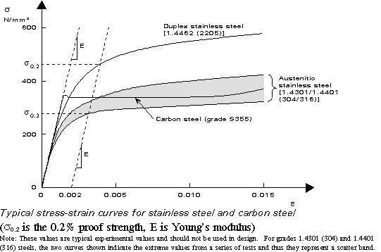
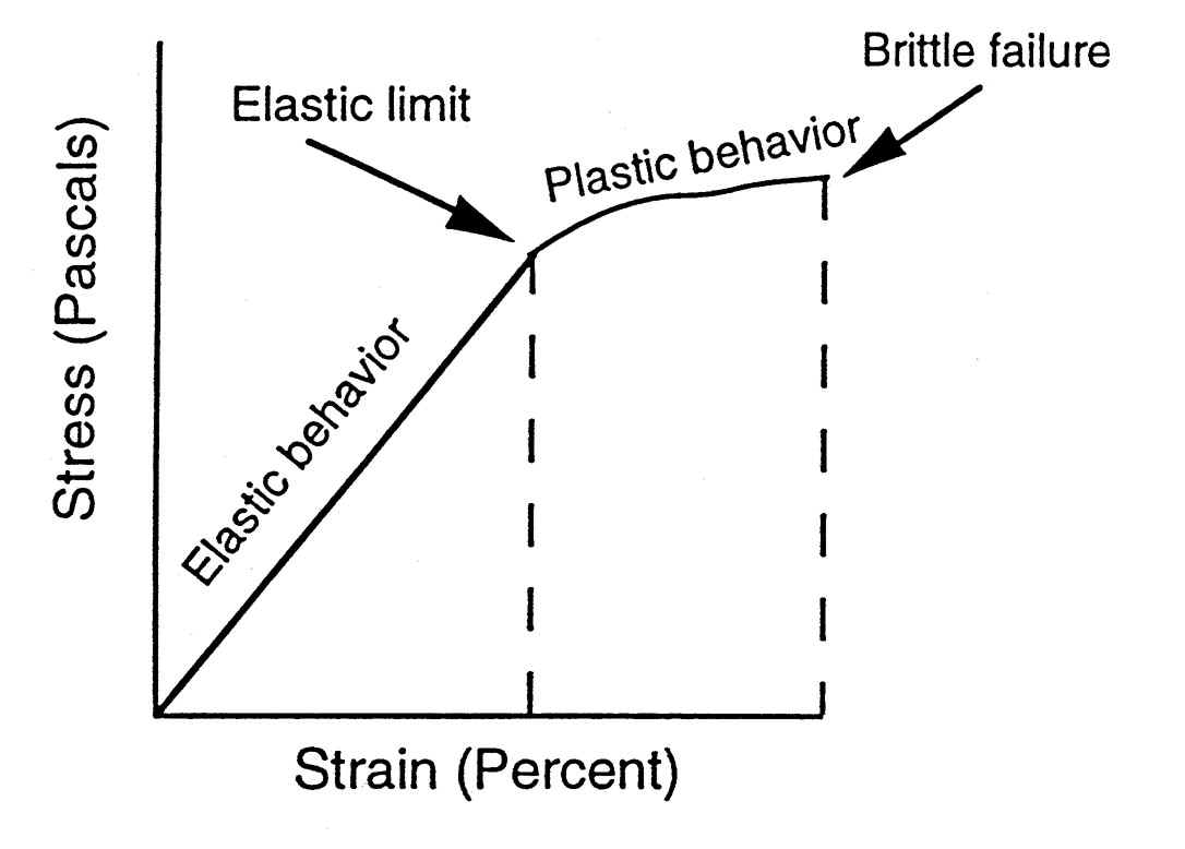
The dislocations move along the densest planes of atoms in a material, because the stress needed to move the dislocation increases with the spacing between the planes. FCC and BCC metals have many dense planes, so dislocations move relatively easy and these materials have high ductility. Metals are strengthened by making it more difficult for dislocations to move.
 The dislocations in plastic deformation
 Transmission Electron Micrograph of Dislocations
 Dislocation in Silicon Crystal


 Alloy Suppliers
  Aluminum
  Aluminum Extrusions
  Copper-Brass-Bronze
  Nickel
  Magnets
  Stainless Steel
  Stainless Steel Tubing
  Steel Service Centers
  Titanium
  Tungsten
  Wire Rope